- 您现在的位置:买卖IC网 > Sheet目录1999 > ICS9E4101AFILFT (IDT, Integrated Device Technology Inc)IC TIMING CTRL HUB PROG 56SSOP
IDTTM
Programmable Timing Control HubTM for Intel Systems
1408A—01/25/10
ICS9E4101
Programmable Timing Control HubTM for Intel Systems
7
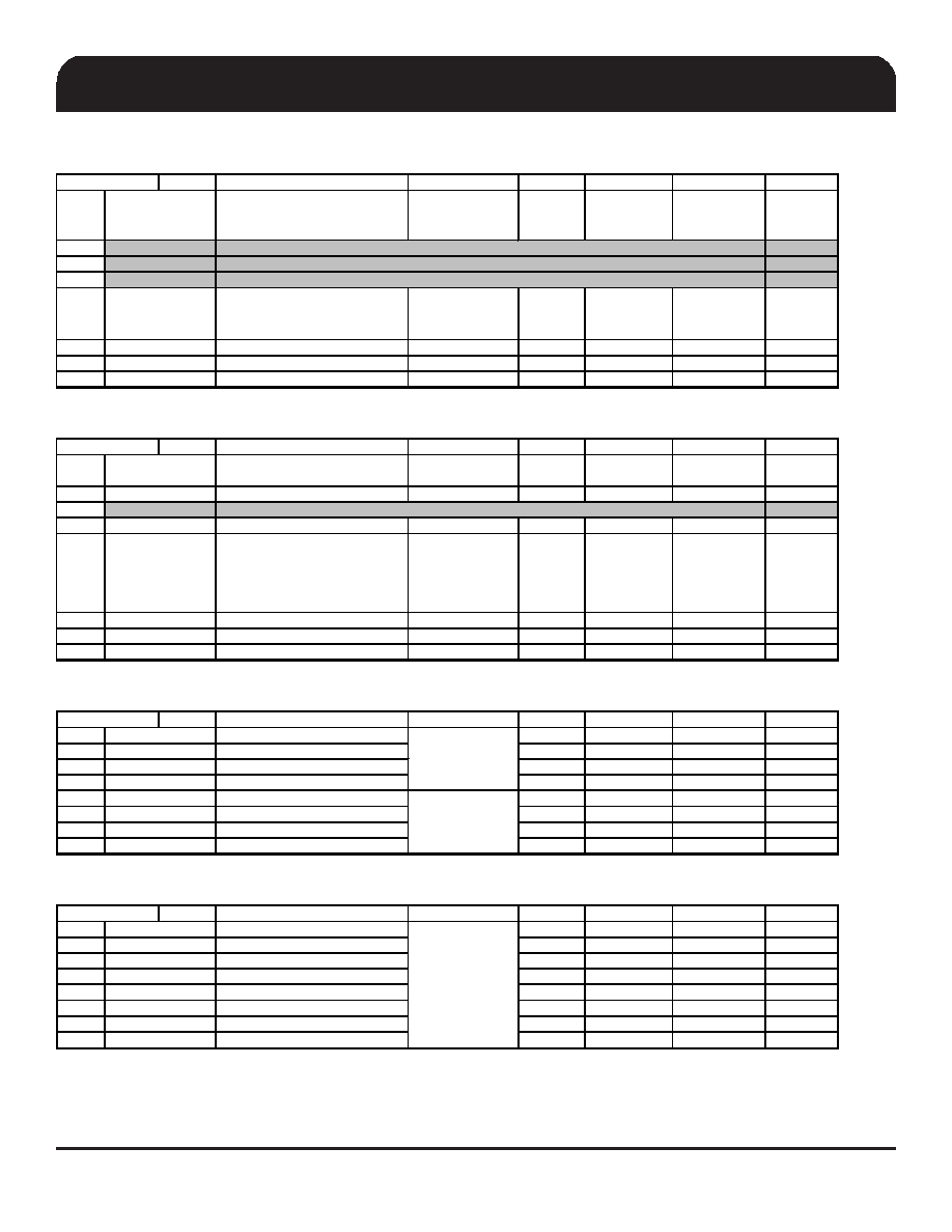
I
2C Table: Output Control Register
Pin #
Name
Control Function
Type0
1
PWD
Bit 7
SRC Stop Drive Mode
Drive Mode in
PCI_Stop
RW
Driven
Hi-Z
0
Bit 6
0
Bit 5
0
Bit 4
0
Bit 3
SRC PD Drive Mode
Drive Mode in PD
RW
Driven
Hi-Z
0
Bit 2
CPUCLK_ITP
Drive Mode in PD
RW
Driven
Hi-Z
0
Bit 1
CPUCLK1
Drive mode in PD
RW
Driven
Hi-Z
0
Bit 0
CPUCLK0
Drive mode in PD
RW
Driven
Hi-Z
0
I
2C Table: Output Control Register
Pin #
Name
Control Function
Type0
1
PWD
Bit 7
Test Mode Selection
Test Mode
Selection
RW
Hi-Z
REF/N
0
Bit 6
Test Clock Mode Entry
Test Mode
RW
Disable
Enable
0
Bit 5
0
Bit 4
REFOUT Strength
Strength Prog
RW
1X
2X
1
Bit 3
PCI/SRC_STOP
Stop all PCI and
SRC clocks
RW
Enabled, all
stoppable PCI
and SRC
clocks are
stopped.
Disabled, all
stoppable PCI
and SRC clocks
are running
1
Bit 2
FS_C
readback
R
-
LATCHED
Bit 1
FS_B
readback
R
-
LATCHED
Bit 0
FS_A
readback
R
-
LATCHED
I
2C Table: Vendor & Revision ID Register
Pin #
Name
Control Function
Type0
1
PWD
Bit 7
RID3
R
-
0
Bit 6
RID2
R
-
0
Bit 5
RID1
R
-
0
Bit 4
RID0
R
-
0
Bit 3
VID3
R
-
0
Bit 2
VID2
R
-
0
Bit 1
VID1
R
-
0
Bit 0
VID0
R
-
1
I
2C Table: Byte Count Register
Pin #
Name
Control Function
Type0
1
PWD
Bit 7
BC7
RW
-
0
Bit 6
BC6
RW
-
0
Bit 5
BC5
RW
-
0
Bit 4
BC4
RW
-
0
Bit 3
BC3
RW
-
1
Bit 2
BC2
RW
-
0
Bit 1
BC1
RW
-
0
Bit 0
BC0
RW
-
0
-
Byte 5
Byte 6
19,20,22,23,
24,25,26,27,30,31,
32,33,35,36
RESERVED
17,18,19,20,22,23,
24,25,26,27,30,31,
32,33,35,36
54,55,56,3,4,5,8,9,
10
19,20,22,23,
24,25,26,27,30,31,
32,33,35,36
35,36
REVISION ID
RESERVED
-
40,41
43,44
52
-
RESERVED
-
VENDOR ID
-
Byte 7
-
Byte 8
-
Writing to this
register will
configure how
many bytes will be
read back, default
is 08 = 8 bytes.
-
发布紧急采购,3分钟左右您将得到回复。
相关PDF资料
ICS9EX21801AKLF
IC FANOUT BUFF DIFF 72-VFQFN
ICS9EX21831AKLF
IC FANOUT/BUFFER DIFF 72VFQFN
ICS9FG1901HKLFT
IC FREQUENCY GENERATOR 72-QFN
ID82C54
IC OSC PROG TIMER 8MHZ 24DIP
IDT2308A-4DCI8
IC CLOCK MULT ZD HI DRV 16-SOIC
IDT2309-1HPGGI
IC CLK BUFFER ZD HI DRV 16-TSSOP
IDT2309A-1HPGG
IC CLK BUFFER ZD HI DRV 16-TSSOP
IDT2309B-1HPGGI
IC CLK BUFFER HIGH DRIVE 16TSSOP
相关代理商/技术参数
ICS9EMS9633BKILF
功能描述:IC EMBEDDED PC MAIN CLK 48VFQFPN RoHS:是 类别:集成电路 (IC) >> 时钟/计时 - 专用 系列:- 标准包装:1 系列:- 类型:时钟/频率发生器,多路复用器 PLL:是 主要目的:存储器,RDRAM 输入:晶体 输出:LVCMOS 电路数:1 比率 - 输入:输出:1:2 差分 - 输入:输出:无/是 频率 - 最大:400MHz 电源电压:3 V ~ 3.6 V 工作温度:0°C ~ 85°C 安装类型:表面贴装 封装/外壳:16-TSSOP(0.173",4.40mm 宽) 供应商设备封装:16-TSSOP 包装:Digi-Reel® 其它名称:296-6719-6
ICS9EMS9633BKILFT
功能描述:IC EMBEDDED PC MAIN CLK 48VFQFPN RoHS:是 类别:集成电路 (IC) >> 时钟/计时 - 专用 系列:- 标准包装:28 系列:- 类型:时钟/频率发生器 PLL:是 主要目的:Intel CPU 服务器 输入:时钟 输出:LVCMOS 电路数:1 比率 - 输入:输出:3:22 差分 - 输入:输出:无/是 频率 - 最大:400MHz 电源电压:3.135 V ~ 3.465 V 工作温度:0°C ~ 85°C 安装类型:表面贴装 封装/外壳:64-TFSOP (0.240",6.10mm 宽) 供应商设备封装:64-TSSOP 包装:管件
ICS9EMS9633BKLF
功能描述:IC EMBEDDED PC MAIN CLK 48VFQFPN RoHS:是 类别:集成电路 (IC) >> 时钟/计时 - 专用 系列:- 标准包装:1 系列:- 类型:时钟/频率发生器,多路复用器 PLL:是 主要目的:存储器,RDRAM 输入:晶体 输出:LVCMOS 电路数:1 比率 - 输入:输出:1:2 差分 - 输入:输出:无/是 频率 - 最大:400MHz 电源电压:3 V ~ 3.6 V 工作温度:0°C ~ 85°C 安装类型:表面贴装 封装/外壳:16-TSSOP(0.173",4.40mm 宽) 供应商设备封装:16-TSSOP 包装:Digi-Reel® 其它名称:296-6719-6
ICS9EMS9633BKLFT
功能描述:IC EMBEDDED PC MAIN CLK 48VFQFPN RoHS:是 类别:集成电路 (IC) >> 时钟/计时 - 专用 系列:- 标准包装:28 系列:- 类型:时钟/频率发生器 PLL:是 主要目的:Intel CPU 服务器 输入:时钟 输出:LVCMOS 电路数:1 比率 - 输入:输出:3:22 差分 - 输入:输出:无/是 频率 - 最大:400MHz 电源电压:3.135 V ~ 3.465 V 工作温度:0°C ~ 85°C 安装类型:表面贴装 封装/外壳:64-TFSOP (0.240",6.10mm 宽) 供应商设备封装:64-TSSOP 包装:管件
ICS9EPRS475BGLF
制造商:Integrated Device Technology Inc 功能描述:IC EMBEDDED PC MAIN CLK 56TSSOP
ICS9EPRS475BGLFT
制造商:Integrated Device Technology Inc 功能描述:IC EMBEDDED PC MAIN CLK 56TSSOP
ICS9EPRS475CGLF
功能描述:IC EMBEDDED PC MAIN CLK 56TSSOP RoHS:是 类别:集成电路 (IC) >> 时钟/计时 - 专用 系列:TCH™, PCI Express® (PCIe) 标准包装:1,500 系列:- 类型:时钟缓冲器/驱动器 PLL:是 主要目的:- 输入:- 输出:- 电路数:- 比率 - 输入:输出:- 差分 - 输入:输出:- 频率 - 最大:- 电源电压:3.3V 工作温度:0°C ~ 70°C 安装类型:表面贴装 封装/外壳:28-SSOP(0.209",5.30mm 宽) 供应商设备封装:28-SSOP 包装:带卷 (TR) 其它名称:93786AFT
ICS9EPRS475CGLFT
功能描述:IC EMBEDDED PC MAIN CLK 56TSSOP RoHS:是 类别:集成电路 (IC) >> 时钟/计时 - 专用 系列:TCH™, PCI Express® (PCIe) 标准包装:1,500 系列:- 类型:时钟缓冲器/驱动器 PLL:是 主要目的:- 输入:- 输出:- 电路数:- 比率 - 输入:输出:- 差分 - 输入:输出:- 频率 - 最大:- 电源电压:3.3V 工作温度:0°C ~ 70°C 安装类型:表面贴装 封装/外壳:28-SSOP(0.209",5.30mm 宽) 供应商设备封装:28-SSOP 包装:带卷 (TR) 其它名称:93786AFT